Optical Link
A High Bandwidth Low Noise Optical VLF Link
This is an article that I wrote which first appeared on Renato Romero’s website vlf.it.
It describes the design, characteristics and use of a high bandwidth, low noise optical system for connecting a VLF receiver to a data sampling system. This easy to build, inexpensive system has a flat response to over 200KHz, and a noise curve well below the VLF band.
“The State Of The Art”
There are a number of alternatives the experimenter can use to connect an ELF or VLF receiver to a data collection system. Each of them has distinct advantages and disadvantages. Before discussing the design criteria used for the optical link, I would like to discuss several of the most popular connection schemes currently in use. This will serve as a good basis for comparison, and will allow the experimenter to evaluate the optical system in context.
-
CABLE. Direct cable connection is by far the most popular method for carrying the signal inside for further processing. It is relatively inexpensive, easy to place, and very durable. Getting far enough away from domestic interference usually requires a significant length of coax or twisted pair cable. With that length comes a very large capacitive load, which can be very difficult to drive properly. In addition to the line capacitance, the cable often acts as an unintentional secondary antenna for the system, bringing in an number of unwanted signals. Worst of all, the cable acts as a current path for the difference in ground potentials between the receiver and the rest of the system, introducing high levels of AC interference. Even if you utilize 1:1 transformers on both ends of your signal line to provide ‘galvanic isolation’, you still aren’t truly ‘isolated’. Every transformer has a (usually) small but finite capacitance between the primary and secondary windings. That capacitance acts as a path for AC signals.
-
DIRECT FM MODULATION. One way of working around the isolation limits of a direct cable connection is to feed the output of the VLF receiver into an FM transmitter. The problem with using an FM modulator is that strong sferics can tend to over-modulate the transmitter, and the FM link itself can add noise and intermodulation. The bandwidth and dynamic range of the FM link can also be a problem, and FM radio links are not completely immune to interference. They can be used very effectively in certain settings, however, like the Schumann receiver built by Sven Nordin.
-
802.11 NETWORK. A way to work around the limitations of direct FM modulation, and preserve the isolation provided by a radio link, is to digitize the signal at the receiver and then forward it via radio. A number of discussions on this topic have occurred on the Yahoo VLF Group list server, and it is also a method I have tried myself. However, when you combine a receiver (say, 12-15ma), a GPS (~90ma), a USB sound card and a Raspberry Pi (or equivalent), your power budget can easily exceed 0.5A. If you don’t live near the equator, it can take a significant investment in solar panels and batteries to make the system completely independent. Also, with the proliferation of 802.11 devices these days, the 2.4GHz and 5GHz bands can be very crowded, causing performance and reliability problems.
Having used all of these methods in various forms, I developed a “wish list” of design criteria for a VLF signal transfer system:
- Low Noise. After considerable time and effort to design, build, and place a receiver, the connection system shouldn’t raise the noise floor above the VLF signal we want to capture.
- Flat Response. The system should not radically re-shape or compress the desired signal.
- High Bandwidth. The link should be capable of passing at least 96KHz, the highest practical reception limit using off-the-shelf sound cards.
- Total Galvanic Isolation. Like the radio systems mentioned above, the link should achieve total galvanic isolation.
- Low Power Consumption. The link should fit easily in the power budget of a conventional ELF/VLF receiver.
- Readily Available Parts. The system should not use exotic or hard to find components.
Optical systems provide the galvanic isolation and high bandwidth we need for such a system, and like radio, provide superb lightning protection. Quite a number of products and circuit designs exist, but all fit neatly into two categories:
Digital. The vast majority of designs or products involve digitizing an analog signal and transmitting it digitally via the optical link. While that is not inherently bad, for accuracy we have to account for the sample rate drift introduced by exposing the A/D converter components (assuming it is externally clocked) to the same temperature swings as the receiver itself. The additional complexity and circuitry at the VLF receiver increase the power budget as well. In most cases the sample rates used limit the bandwidth to the audio range, usually stopping between 20-25KHz.
Analog. The remaining systems were kits designed to send analog audio between two points. After building a number of these, I was unable to find a design that didn’t inherently limit the frequency response, or, had a flat response over the pass band. All had high levels of noise, which made them unsuitable for use in a VLF system.
After some consideration, it seemed the simplicity and low cost of the analog solutions were more in harmony with design criteria I wanted to meet. The limitations of the existing kits, however, required a “fresh start.”
The system developed in this article avoids the complexity of a digital optical system, and has a flat response to analog signals up to 200KHz. The measured noise is well below the signal of interest, and the system is inexpensive, quite easy to build, and use in the field.
System Design
After creating, analyzing and testing a number of designs, several points became very clear:
-
Attempting to frequency modulate the signal creates the complexity we’re trying to avoid: wide-range VCO (and its temperature stability problems), finding or building a PLL with a large enough lock range, PLL loop bandwidth limits, and phase noise.
-
The solution should use closed coupling to the media (like a fiber) to avoid external noise
-
Photo emitters and receivers have a number of non-linear characteristics, which are dependent on the mode in which they are used (voltage vs current), and the optical intensities employed (non-linear portions of response curves.)
-
Phototransistors tend to have higher junction capacitance than photodiodes. Given the bandwidth-limiting effects of that junction capacitance, a photodiode is preferred in the receiver.
-
The photo emitter wavelength and detector peak sensitivity wavelength do not have to be perfectly matched.
Given these experiences, I chose amplitude modulation of the optical signal, with a photodiode as the optical detector. A review of the literature quickly showed that using the photodiode current response is more linear (often, better than 1%) than the corresponding voltage response. The literature also showed that using a transimpedance amplifier in the receiver would allow linear conversion of the diode current to an output voltage.
A transimpedance amplifier (TIA) is a current to voltage converter, which can be used to amplify the current output of sensors and detectors. A simple, idealized transimpedance photodetector is shown below in Figure 1. It is typically constructed with an operational amplifier. In this case, the transimpedance op-amp presents a low impedance to the photodiode and isolates it from the amplifier output. The current induced in the photodiode by optical input is a reverse current, and is converted to an output voltage through the active feedback of the op-amp and resistor Rf .
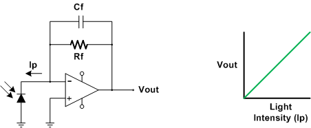
Figure 1: Idealized Transimpedance Amplifier
The op-amp is configured as an inverting amplifier, and therefore the gain is Rf (ignoring the effects of Cf for the moment). Therefore:
[1] Vout = Rf x Ip .
In reality, photodiodes have a finite junction capacitance, which becomes important when calculating the noise and frequency response of the transimpedance amplifier. A more appropriate model is shown in Figure 2, below, and will be used as the basis for further analysis and simulation.
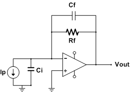
Figure 2: A better model
Where
- Rf = Feedback resistor (sets receiver gain)
- Cf = Feedback shunt capacitance which helps reduce noise (but limits bandwidth)
- Ci = Junction capacitance of photodiode detector
- Ip = Photocurrent induced in photodiode.
A number of circuit properties can be derived from these quantities, but it is well beyond the scope of this article. The reader is encouraged to examine the references at the end for a more in-depth treatment of transimpedance amplifier performance and characteristics.
To begin this design, we will determine the amount of gain, and therefore the minimum Rf required.
Given photodiode responsivity Resp (λ), which is the device response to optical input power Pin , equation [1] above can be rewritten:
[2] Vout = Pin x Resp (λ) x Rf
Using this equation, we can begin to estimate the value of Rf , for a given photodiode and incident power Pin .
While evaluating kits, and testing numerous emitters and detectors, I came across a product line from Industrial Fiber Optics, Inc. The IF series of emitters and detectors have a number of electrical and mechanical characteristics that make them ideal for this application. After a number of basic bench experiments with their products, the IF-E96 660nm LED transmitter and IF-D91 photodiode detector were selected, based on device bandwidth and the availability of relatively inexpensive 1000um fiber that worked with both devices.
In my particular application, the linear distance between the VLF receiver and data acquisition system was approximately 120 feet (36m.) Industrial Fiber Optic’s 1000um fiber is available in any length, but was readily available in a 165 foot (50m) length from Digikey, so that length is used as the basis for this design. Please refer to the construction section below for more information about this fiber.
The relationship between IF-E96 output intensity and forward current is linear for sufficiently high If , as shown by the following chart from the data sheet:
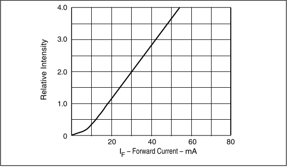
Figure 3: IF-E96 Relative Intensity vs Forward Current
In practice, based on measuring a small set of IF-E96s, the linear region begins just above 5-6ma forward current.
The IF-E96 datasheet specifies that with If = 20ma, it couples 200uW into a 1000um fiber placed directly against the output lens. In order to conserve current use in the optical transmitter, and to estimate a lower bound for Pin , we will assume If = 10ma, and Pout = ~100uW in our optical transmitter. In order to relate the voltage presented to the transmitter to Pin and Rf in the receiver, we will assume 1V will result in 10ma If (equivalent R of 100 ohms), which means that:
[3] Pout (uW) ≅ 100 x Vin (V).
The IF-E96 is designed to mate with SH-4001 1000um optical fiber. The SH-4001 data sheet lists the optical attenuation at 650nm to be between 190dB/km and 210dB/km, depending on temperature, and assuming no significant bends. This translates into approximately 10.5dB (210db/km), for the 50m fiber in this design.
Therefore, if Pin is the power we expect to be received by the photodiode,
10 Log10 ( Pout / Pin ) = -10.5 dB, or
[4] Pin = 0.089125 x Pout , and combining with [3],
[5] Pin = 8.9125 x Vin
The responsitvity Resp (λ) of the IF-D91 is given as 0.4uA / uW at 632nm. Using this as an approximation for 660nm, we see from [2] and [5] that
Vout = Pin x Resp (λ) x Rf =8.9125 x Vin x 0.4uA x Rf
If we want unity gain for our link, or Vout = Vin , we set Vout = Vin = 1V, and solve for Rf :
1 = 8.9125 x 1 x 0.4x10-6 x Rf , or Rf = 280k.
In practice, Rf will likely be much higher due to imperfections in the fiber ends and imperfect alignment with the transmitter and receiver. According to the SH-4001 data sheet, bends in the fiber can add additional attenuation (0.5dB for each 25mm radius bend). Since the fiber will undoubtedly follow several corners, and there will be some loss due to imperfect mating with the transmitter and receiver, we will add an additional 1dB loss for bends, and 2-3dB for mating, raising the total attenuation to 13.5 - 14.5dB. This gives us a final working Rf value of 550k - 700k. It should be noted that it is not uncommon for Rf to approach or exceed 1M in this type of receiver.
Now that we have derived a working range for Rf , our next task is to select an op-amp for our design that will provide at least 100kHz bandwidth, and that minimizes the noise in the optical receiver.
From Graeme(1) and Gallant(2), for a transimpedance amplifier:
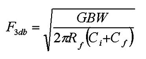
For the IF-D91, Ci = 4pF. Assuming a minimal initial value for Cf , 1pF, we can determine the F3db frequency for a range of popular low current noise or low voltage noise op-amps. This set of op-amps was chosen because of their availability (one of our requirements), and the availability of the necessary data for our model. Given that our value for Rf is simply an approximation and will likely change in practice, using the equation above we can examine the F3db for a range of Rf values:
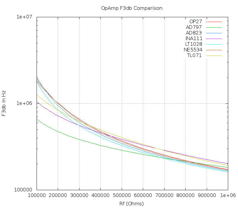
Figure 4: Op-amp F3db with respect to Rf.
We can see that all of them easily exceed our design goal of 100kHz, and there is no clear choice. Next, we examine each op-amp for its noise characteristics in this circuit. From Gallant(2), we see that the noise voltage at the output of a transimpedence amplifier is usually dominated by the op-amp input noise voltage contribution. However, the op-amp current noise contributes noise voltage through Rf , and Rf itself contributes thermal noise. In order to determine which op-amp would generate the lowest overall noise in this application, we need to simulate the noise for each.
Using the approximations from Gallant(2),
- in = op-amp input current noise in fA/√Hz
- vn = op-amp input voltage noise in nV/√Hz
- GBW = op-amp gain-bandwidth product in MHz
- Rf = Feedback resistor in Mohms
- Cf = Feedback capacitor in pF
Vnoise (Rf ) = √(4Kb TRf ), where T=293K
Vnoise (in ) ≅ in x √( Rf / (4 x Cf ))
Vnoise (vn ) ≅ vn x √( pi/2 x ((Cf +Ci /Cf )) x GBW )
Vnoise (total) = √( Vnoise (Rf )2 + Vnoise (in )2 + Vnoise (vn )2 )
It should be noted that this model does not calculate the noise density, but rather a total noise voltage across the bandwidth of the op-amp. Using this value will allow us to choose an op-amp based on the lowest total noise value.
Setting Ci = 4pF (per data sheet), and assuming a minimal value for Cf , 1pF, we can simulate the total system noise for our set of op-amps:
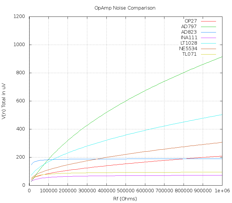
Figure 5: Op-amp Total Noise Comparison. Click for larger image.
Transmitter
IF-E96 at If
≅ 10ma
Cable
50m of SH 4001 1000um optical cable
- Rf = 550k to 700k
- Cf = 1pF
- Ci = 4pf (using the IF-D91 as receiver)
- Op-amp = TL071
Circuit Operation
The transmitter circuit is shown below in Figure 6. C1 couples the incoming VLF signal to U1, an OP27. U1 is configured as a unity-gain non-inverting summing amplifier which adds an offset voltage from RV1 to the incoming VLF. The DC offset voltage from RV1 causes the output of U1 to follow the same DC offset, which controls the average forward current through R1 and D1, the LED transmitter. The OP27 was also chosen for its excellent output current capability, and low input noise. As mentioned in the previous section, placing the LED in a linear region of its’ current-intensity response curve is important to the proper operation of the the link. For the IF-E96, the beginning of that linear region occurs at approximately 5-6ma forward current. For initial testing, the non-inverting input of U1 will be offset at approximately 2.75V, resulting in 10ma through R1 and D1 (assuming 1.7-1.8V forward voltage on D1, as per the data sheet). This offset also allows the the input signal to amplitude-modulate the optical output of D1 by changing the voltage sum on the non-inverting input of U1.
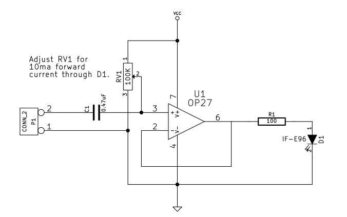
Figure 6: Optical Transmitter
The receiver is a transimpedance amplifier like the idealized circuit shown in the previous section, with the component values we have calculated placed into the circuit:
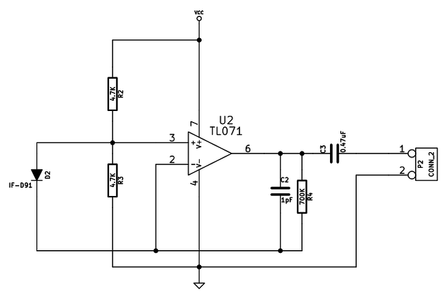
Figure 7: Optical Receiver
As discussed in the previous section, U2 is configured as a transimpedance amplifier. One small addition is the voltage divider R2 and R3, which provides an artificial ground reference at 1/2 Vcc for U2. The values for R2 and R3 are sufficiently low that they do not make a meaningful contribution to the noise of the receiver, but sufficiently high that they do not unnecessarily raise the current consumption of the receiver. D2 is connected across the input terminals of U2, and the current induced in D2 by optical input is amplified and coupled to the output via C3. R4 is equivalent to Rf in the previous section, and controls the receiver gain. In this implementation, the optical cable is 164 feet (50m), and a 700K resistance was required to achieve approximate unity gain for the entire link. C2 is an actual, discrete ceramic capacitor, and does not represent stray capacitance. When this circuit was initially constructed on a breadboard, the traces provided C2. When the receiver was the built as a prototype, I had to add C2 to stabilize the circuit and eliminate distortion. C2 may be increased to further reduce noise (which as we shall see, is not necessary) at the expense of bandwidth.
The prototype was constructed using prototyping PC board enclosed in aluminum Hammond enclosures, to shield the circuits electrically and optically. One advantage of the IF series from Industrial Fiber Optics is that the LED transmitters and photodiode receivers come in a rugged plastic enclosure that allows them to be easily anchored to the circuit board. There is also a screw-compression fitting on each device, which makes connecting and disconnecting optical fiber very easy (please refer to the data sheets for more mechanical details). The optical fiber is also easy to prepare: a flat cut, made at 90 degrees to the cladding with a sharp utility knife is all that is required - no polishing, no chemicals. The photos below show the construction details:
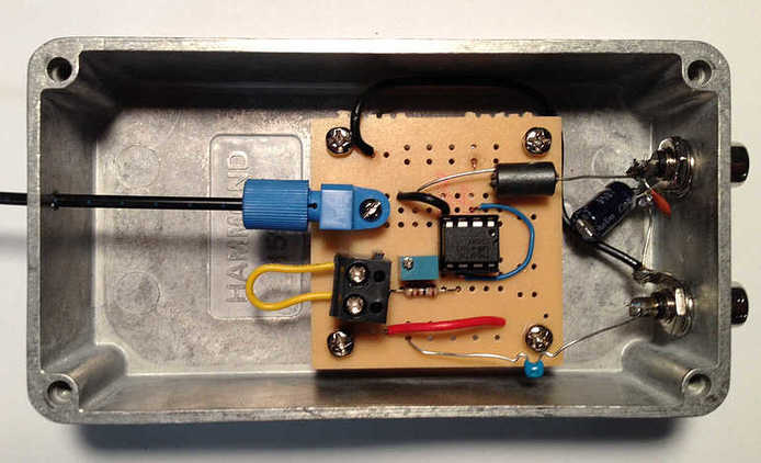
Photo 1: Optical Transmitter
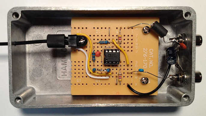
Photo 2: Optical Receiver
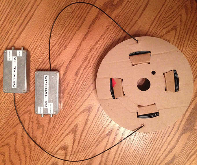
Photo 3: Fiber Spool with TX and RX attached
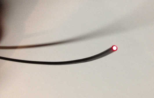
Photo 4: 1000um fiber illuminated by TX
The wire loop and terminal block in the transmitter (photo 1) is my way of easily interrupting the circuit between U1 and the IF-E96 to set or measure If . The extra components seen near the RCA connectors on both the transmitter and receiver are power filtering components (100uF, 0.1uF, VK200) placed there out of habit, rather than necessity. They are not required to achieve the performance shown in the following section. For the performance and noise tests, I left the fiber on the spool as it came from Digikey (photo 3). The bend radius of the spool is approximately 80mm, and represents a good test for the link by causing extra attenuation.
Link Performance
In order to test the frequency response of the link, I used RMAA with an ASUS Xonar D1 192kHz sound card:
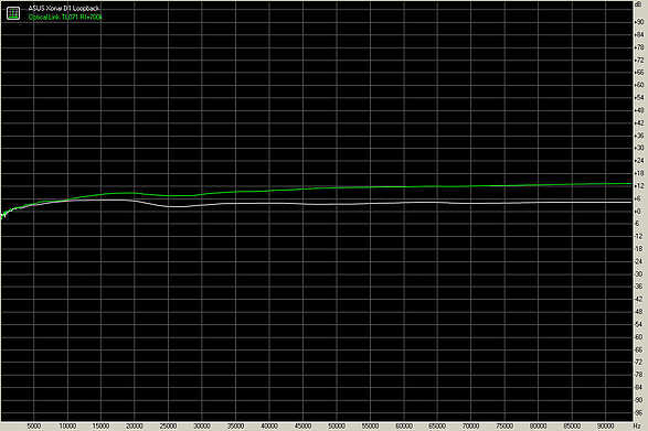
Figure 8: Link Frequency Response vs Soundcard
The white trace shows the frequency response of the sound card, 1-96kHz, using a swept sine and a loopback cable. It should be noted, like almost all sound cards, that the response curve is not perfectly flat. The response of the optical link is shown in green. As shown, the response of the link is quite flat with respect to the native response of the sound card. Additional tests with a signal generator and oscilloscope show a flat response out to 200kHz, with an upper F3db at approximately 275kHz, which meets our design criteria and agrees with our simulation results in Figure 4. The lower F3db was measured at approximately 15Hz. The link will pass lower frequencies, with a corresponding drop in amplitude.
In order to evaluate the noise performance of the link, the following measurements were made using the vlfrx toolchain:
- The noise floor of the ASUS Xonar D1, used in the receiving system, with both inputs shunted with 50 ohm resistors
- The system noise floor with the optical link connected, transmitter input shorted, using a TL071CN in the receiver
- The system noise floor with the optical link connected, transmitter input shorted, using an OP27 in the receiver (to test noise model)
- VLF spectrum sample, using the optical link
With these measurements, we can compare (4) with the noise floors (1-3), and determine if the optical link is usable in VLF reception.
The measurements are summarized in the following graph:
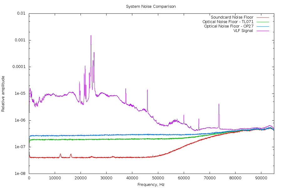
Figure 9: System Noise Floor Comparison.
As shown in Figure 9, the noise floor for the optical link using the TL071 (green trace) is well below the VLF signal of interest (purple trace). As predicted by the model, the noise performance of the OP27 (blue trace) is not as good as the TL071 in this application. It is still well below the VLF signal, however, and could also be used in the receiver. Note that it is pin-compatible with the TL071, and is an easy swap.
The upward tilt of the noise floor on the ASUS Xonar D1 is similar to that of other 192kHz audio cards, such as the M-AUDIO Audiophile 192, and poses a lower limit on signal strength for signals > 80kHz. This is an artifact of my reception system, and not the optical link itself.
At 12V, the supply current for the transmitter is 13ma with If set to 10ma, and is easily powered by the same power supply as the VLF receiver (battery, etc.) The receiver uses approximately 5-6ma with a high impedance load (like a sound card.)
With a 2.75V bias in the transmitter, the upper limit on input voltage was measured to be 0.8Vrms . Higher amplitudes introduce noticeable distortion. Using 0.8V as our upper limit, and Vnoise (total) for the TL071 as our lower limit, we can calculate the dynamic range:
20 Log10 ( Vmax / Vmin ) = 20 Log10 (0.8/ 93.47x10⁻⁶ ) ≅ 79 dB.
If required, the bias in the transmitter can be raised to further improve the dynamic range. As an example, at 4.5V bias (If ≅ 28ma), the link will accommodate a 2Vrms signal. The dynamic range then becomes:
20 Log10 ( Vmax / Vmin ) = 20 Log10 (2/ 93.47x10⁻⁶ ) ≅ 87 dB.
Practical Considerations
The SH 4001 PMMA fiber used in the construction of this link is remarkably resilient. It can withstand rough handling, repeated flexing (over 10,000 cycles), tight bend radii (25mm), and still function without significant attenuation. I have accidently stepped on the fiber with no significant impact on performance. The jacket on the fiber is made from polyethylene, and while polyethylene is used in a number of direct burial products, I have not been able to determine the effects of direct burial or prolonged exposure to UV light (e.g. sunlight.) There are a number of inexpensive, flexible tubing types available at home improvement stores that would make suitable shields if this is a real concern. Small diameter PVC pipe could also be used.
One other practical consideration in long-term use of the optical receiver is long-term operation without re-introducing all of the AC mains noise we are trying to eliminate. While battery operation is feasible at 5-6ma, it is more convenient to use a mains connected supply. In my implementation of this system, I am using a popular (but noisy) linear regulator, followed by a capacitance multiplier and L/C filtering. While there are many, many more appropriate solutions, this circuit adheres to the “readily available” and “cheap” design requirements.
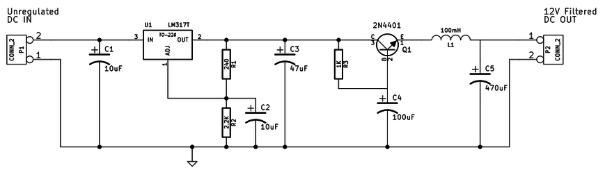
Figure 10: Optical Receiver Power Supply
U1 is an LM317, and is configured as a standard voltage regulator, regulating the DC input to approximately 12.7V. Q1, R3 and C4 form a “capacitance multiplier”, and dramatically reduce the noise output from U1. A more detailed discussion and noise analysis of this circuit can be found here. L1 and C5 form a final filter that eliminates most of what remains of any AC hum and it’s harmonics.
In use, I tie the ground and chassis of this power supply to the PC chassis of my data sampling system, which is also grounded. Due to the low noise output of this supply, and the power supply noise rejection of U2 in the receiver, there is no appreciable injection of mains noise into the VLF signal.
Customizing / Enhancing The Link
There are a number of customizations and enhancements that can easily be made to this link depending on the application:
Input Voltage Range. The RMS voltage from my VLF receiver output is typically 0.1-0.2 V, with much higher spikes on strong sferics. If the transmitter is going to be coupled to a receiver with larger output voltage swings, raising the value of R1 and adjusting RV1 for a higher DC bias will accommodate larger input signal swings.
Increased Link Length. The link as described in this article should be usable to at least 75m by increasing feedback resistor Rf , and if needed, increasing If by adjusting RV1 for a higher DC offset. The IF-E96 660nm LED used in the transmitter is rated for applications of 250ft (75m) by the manufacturer. The link could be extended to over 500ft (150m) by switching to an IF-E93 530nm device, as that wavelength is less attenuated in the PMMA fiber. An increase in Rf will also be required, as the sensitivity of the IF-D91 to 530nm is significantly less than 660nm. It is recommended that the TL071 be used in the receiver in these cases, as the increase in receiver noise is very minimal for increasing Rf (examine gold trace in Figure 5).
Hybrid Systems. The optical link can be used as the first segment of the link between VLF receiver and the data sampling system. This would avoid the “secondary antenna” effects of direct cable connection, and provide all of the benefits of true galvanic isolation (such as for lightning protection). The optical receiver could easily be powered by DC injection into the cable.
References
- Photodiode Amplifiers, Jerald Graeme, McGraw-Hill, 1996
- Transimpedance Amplifiers, Michel I. Gallant Ph.D., http://www.jensign.com/transimpedance/index.html
- Industrial Fiber Optics, Inc.
- IF-E96 Data Sheet
- IF-D91 Data Sheet
- SH 4001 Fiber Data Sheet
Acknowledgements
I would like to thank Tom Becker and the other reviewers, who wish to remain anonymous, for taking the time to review this article. Any errors that remain are completely my own. I owe many thanks to Renato Romero for writing his book and getting me started with VLF in the first place, Paul Nicholson for his truely excellent vlfrx-tools, and the Yahoo VLF_Group for providing years worth of good reading, analysis, and ideas. It is very, very appreciated.