Three Channel Counter
The ionosphere and geophysics have always been “hobbies” of mine. Recently, I began a project to build a 3-axis magnetometer. The first iteration of this project uses FG-3+ fluxgate sensors available from FG Sensors. These sensors are very similar to the sensors once produced by Speake & Co (long out of business). The FG-3+ sensors output a variable period square wave based on the magnetic field strength and direction. The frequency of this square wave typically ranges between 40kHz to over 120kHz.
Requirements
Here are the requirements I began with:
- Three independent channels (X, Y & Z)
- Very accurate gate timing (to reduce this source of measurement error)
The most straightforward approach (or so I thought) would be to use a microcontroller with three timer/counter channels. However, the highest frequency of interest is well over 16 bits (65,536/sec max). Using sub-second gate times introduced error rates that I was not willing to accept. Cascading counters in some microcontrollers could get you 24 or 32 bits, but you end up short of resources to support three channels. Even with enough counter bits, achieving very accurate gate timing (driving the uC with GPS locked clock, or at least an ovenized crystal), and dealing with instruction execution timing, made this approach more than I cared to take on. My requirements now looked like this:
- Three independent channels (X, Y & Z)
- Very accurate gate timing (derived from GPS, to reduce measurement error)
- Discrete components (no uC I could find fit the requirements)
- A Processor independent interface (which really comes from the requirement above)
Due to problems accurately measuring the period of the input signal (see here), I decided to measure the frequency instead. A search for 24bit or 32bit counter/timer chips introduced me to the 74LV8154. This chip is a 32 bit counter, with conservative speed ratings between 25MHz and 40MHz. (TIP: This chip will go much, much faster. Here is a link to a frequency counter using the 74LV8154 that is capable of measuring over 100MHz - without a pre-scaler. My design can easily measure over 30MHz on each channel, and that rises to over 100MHz if you remove or bypass the input inverters.) There is also another interesting clock calibrator project that also uses the 74LV8154.
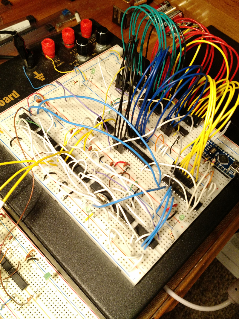
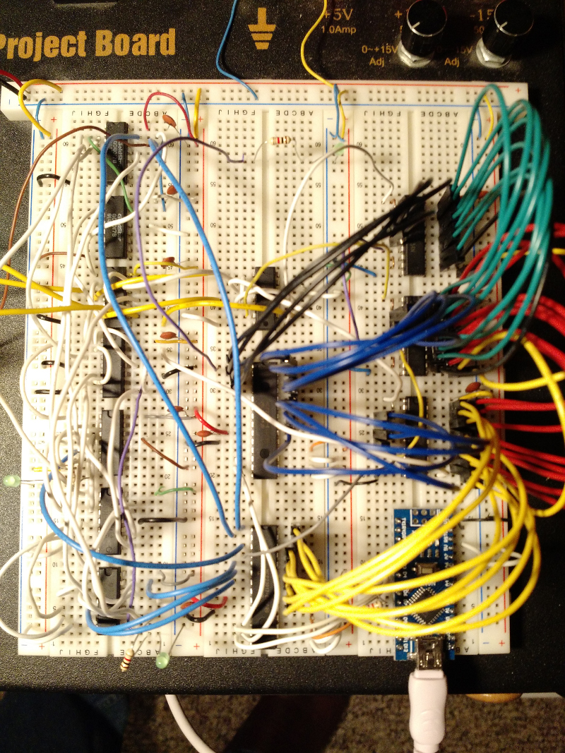
The Prototype
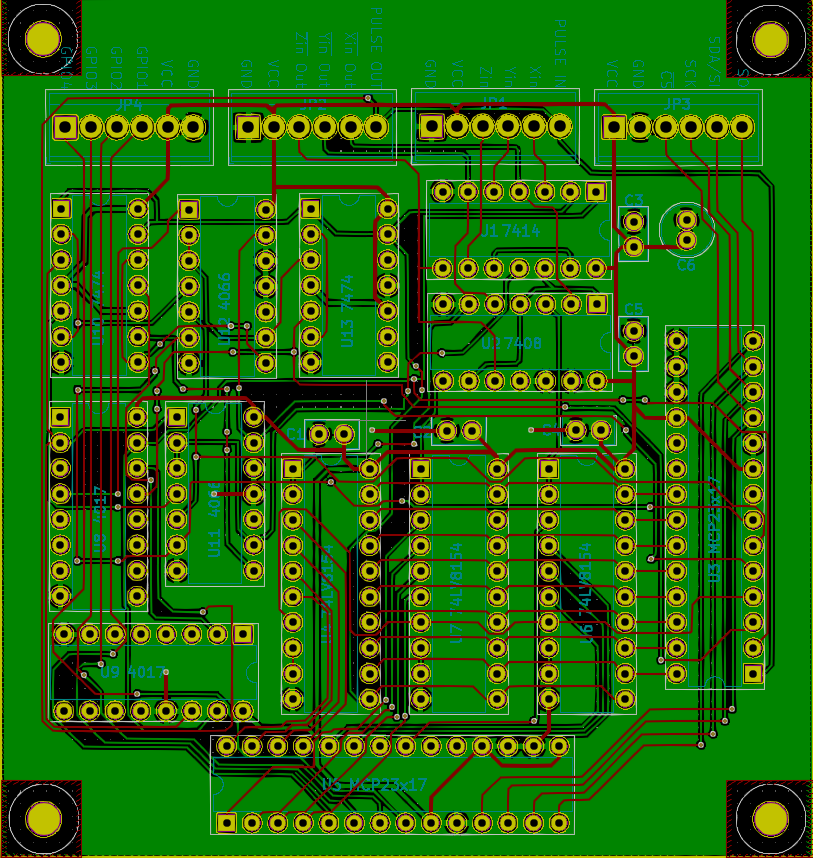
..I settled on the following design (click here for a higher quality PDF):
Circuit Description
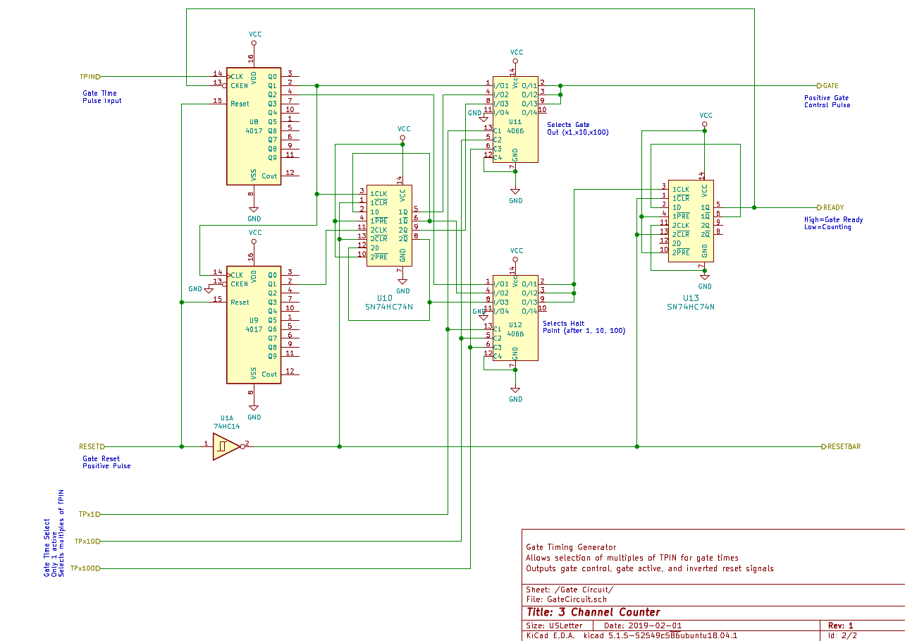
U8-U13 make up the gate control circuit. There are 5 input signals to the control the gate: TPIN, RESET, and TPx1, TPx10, TPx100. TPIN is an active high “time pulse” signal input. To minimize error, TPIN should be derived from a GPS module or ovenized crystal. Active high control lines TPx1, TPx10, and TPx100 select the gate interval in multiples of TPIN. For example, if TPIN is 1Hz, then selecting TPx1 results in a 1 second gate. TPx10 selects a 10 second gate. TPx100 selects a 100 second gate. There is no strict requirement that TPIN is 1Hz. TPIN could for example be 10Hz - in which case you could get 1/10th sec, 1 sec, and 10sec gate times. The longer gate times are useful for ‘averaging’ 10 or 100 counts together. By counting across a larger time period, and then dividing by 10 or 100, you minimize the +/- 1 count error that comes from a phase difference between the input signal and TPIN (see here for a description of the +/- 1 error). RESET is an active high signal that resets the gate circuitry (and later in the chain the counter circuitry) to zero-state. U8 & U9 are used to divide TPIN by 10 and 100. U10 is used to ‘stretch’ the pulse across it’s entire gate time as U8/U9 count. U11 routes the selected active-high gate signal to the GATE output. U12 routes the active-high READY signal from the counters to U13, which generates an active-high ‘ready’ signal used to tell the processor that a count cycle is complete.
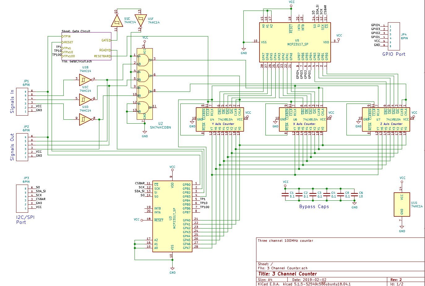
The three input signals are cleaned up by the Schmitt trigger inverter (U1). U2 acts as an input signal gate, which is controlled by the GATE signal from the gate circuit. U4, U6, and U7 are 32 bit counters which count the X, Y, and Z input signal pulses. Each 74LV8154 contains 4 8bit registers that represent the total count value. U5, an I2C GPIO chip, creates the addressing signals to read each register out of each counter chip in turn. U3, another I2C GPIO chip, reads the data lines from each counter chip, and also provides control signals (RESET, TPx1, TPx10, TPx100) for the gate circuit. U3 also allows the controlling processor to read the READY signal from the gate circuit. Four spare GPIO lines from U5 are made available for other, application-specific uses.
Operation
The uC uses U3 to select the desired gate period, then waits for the PPS (TPIN) to go high, then watches for it to go LOW (1 full pulse). The uC then issues a RESET to the counter board via U3, so that the counters begin counting on the next rising edge of TPIN. Once a full count cycle is complete, READY is asserted, and the uC can then use U5 and U3 to read out each 8 bit register from each 74LV8154, and construct 3 32 bit values - one for each input signal.
Sample driver code to operate the board via I2C is here. You will need to supply your own I2C routines for non-AVR processors. If you are using an AVR, contact me and I will supply you with a working code set and an image you can burn onto a Nano to operate this board.
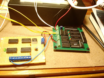
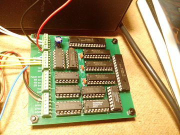
Here are some shots of the board under test (using a non-ovenized crystal). The crystal can be replaced by a GPS module in the magnetometer:
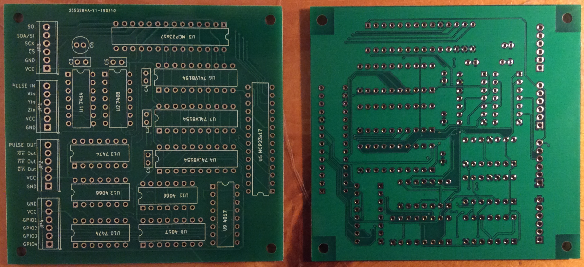
PCBs
I’m sure I could get a much smaller board using surface mount, but I really like the easy construction using through-hole components. Notice that I have made the ‘cleaned’ input signals (post Schmitt trigger) available as /Xin, /Yin, and /Zin, so that the input signals can be chained to other circuitry if desired. There is also a PPS (TPIN) output for use by other circuits. You can modify the board for use with SPI by cutting the “/CS” trace to the second MCP23S17, and running a ‘bodge’ wire from the board to the uC. See here for more information on using multiple SPI chips on the same SCK and SI/O lines. Both the Gerber files and spare boards are available. If you are interested in making your own with the Gerbers, or just buying a PCB, please contact me.